Signal and Power Integrity
Why performing Signal Integrity simulations?
By Austin Lesea, Xilinx, Inc. 2005.
Try and error and rules of thumb are not successful at Multi-Gigabit design anymore. Those days are gone forever.
You’re tired of making PCBs over and over and still not having them work?
Seriously, without simulating all signals, as well as power and ground, you risk making a PCB that will just not work.
You’re tired of being late to market and watching your competition succeed?
Every time you have to fix a problem with a PCB, it necessitates a changed layout, a new fabrication and another assembly cycle. It also requires the re-verification of all parameters. Taking the time to do these things right has both monetary and competitive disadvantages.
You’re tired of spending all this money, only to scrap the first three versions of PCBs and all of the components that went with them?
See reason above.
Your eye pattern is winking at you like this?
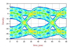
If the eye pattern of a high-speed serial link is closing or closed, it’s likely that the link has a serious problem. You must simulate every element of the design and the complete link to assure an error-free channel.
You cannot meet timing and you are unable to find out why.
Poor signal integrity is the primary cause of adding jitter to all signals in the design. Reflections, loss, crosstalk and Ground bounce are all conspire to add jitter.
The EMC / EMI test fails every time you test a board.
Radiated RF emissions, as well as susceptibility to RF sources, are a sign of poor SI practices.
Your choice is simple: let simulate and get a first pass successful PCB